With Apple’s company use of wireless charging technology on the iPhone 8, it is ignited the entire industry. As an ordinary consumer, in addition to using wireless chargers every day, do you know how does wireless charger be manufactured? Now we are taking the processing process of a wireless charger. Follow us my footsteps and I’ll show you the production process of wireless charging at Lantaisi’s workshop .
Wireless charging is divided into two parts: internal circuit board and external component. The production process of wireless charging will also be introduced in detail from these two sides.
First, Our sales and his customers communicate with each other to determine product design and performance requirements. Next, the technical department of Lanaisi will design the internal circuit board, and the product department will design the shell structure.
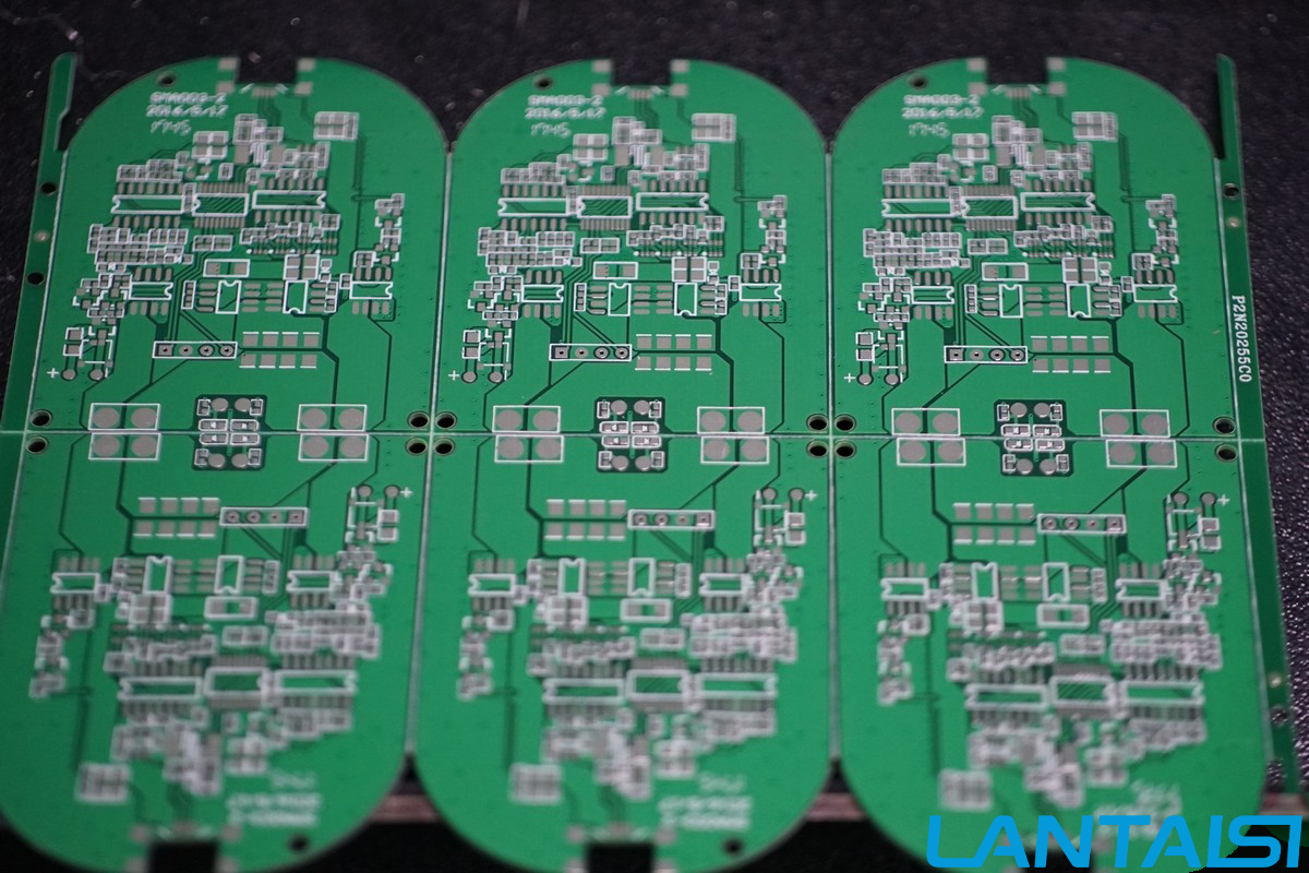
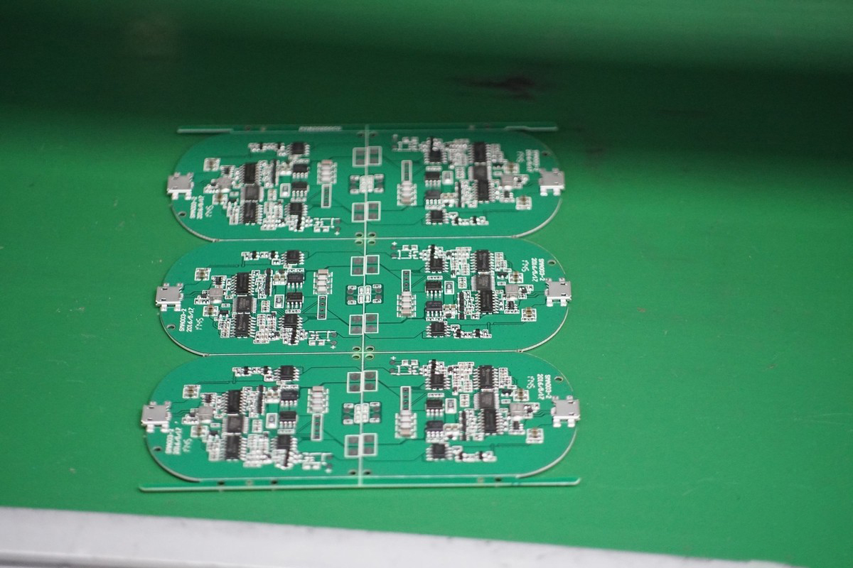
Step 1 : The above picture is a blank board without any electronic components. First, it will be placed on a fully automatic printing machine and painted with a layer of solder paste. The solder paste is mixed with solder powder, flux, and other surfactants and thixotropic agents. It can be seen from the picture that this wireless charger circuit board has more than 30 components.
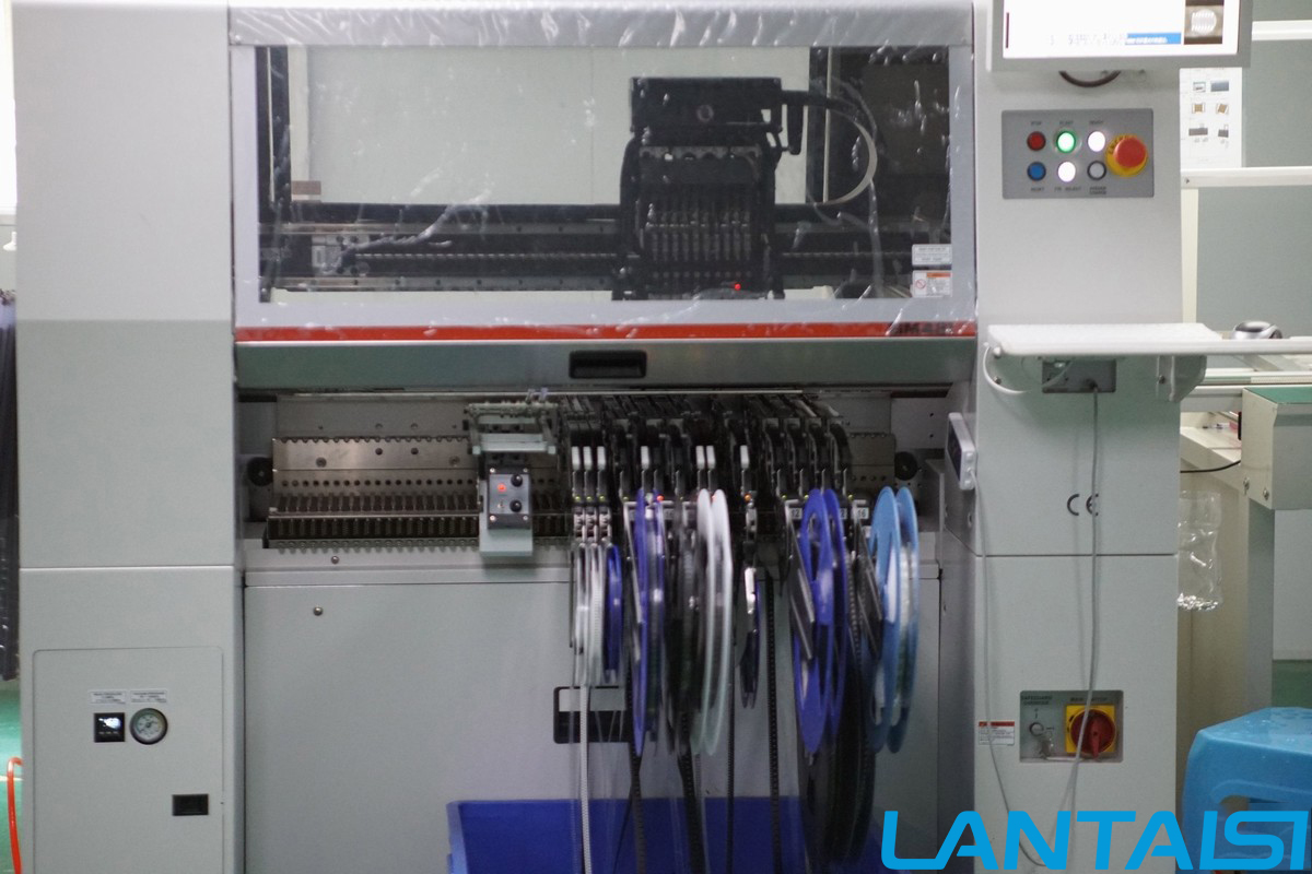
(The picture above shows a fully automatic printing machine.)
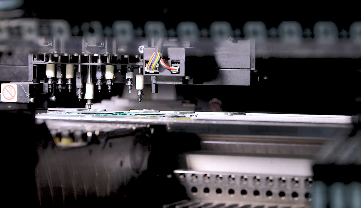
Step 2: Then enter the next process: SMT patch. SMT stands for surface mount technology and is widely used in the electronics industry. It is mainly used for the installation of electronic components with no leads or short leads.
Step 3 : The SMT placement machine installs and fixes the chips, resistors, capacitors, inductors and other components on the circuit board brushed with solder paste in order. Each SMT high-speed placement machine will be controlled by a small computer. Engineers will design and program the preset operating procedures according to the material of each wireless charging circuit board, which greatly improves the placement accuracy of the circuit board.
Step 4 : The picture above shows the reflow soldering operation of the lead-free environmental protection process. The one on the right is the reflow soldering equipment with an internal temperature of more than 200 degrees. The PCB substrate after brushing, patching, and reflow soldering has become a complete PCBA. At this time, the PCBA needs to be inspected to determine whether the functions of each part are normal.
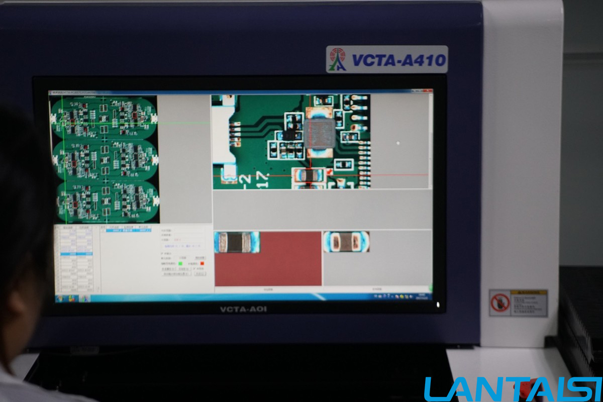
Step 5 : The above picture shows the use of AOI automatic optical detector to inspect PCBA. Through tens of times of magnification, you can graphically check whether there are any problems such as false soldering and empty soldering during the chip and resistance-capacitance placement process.
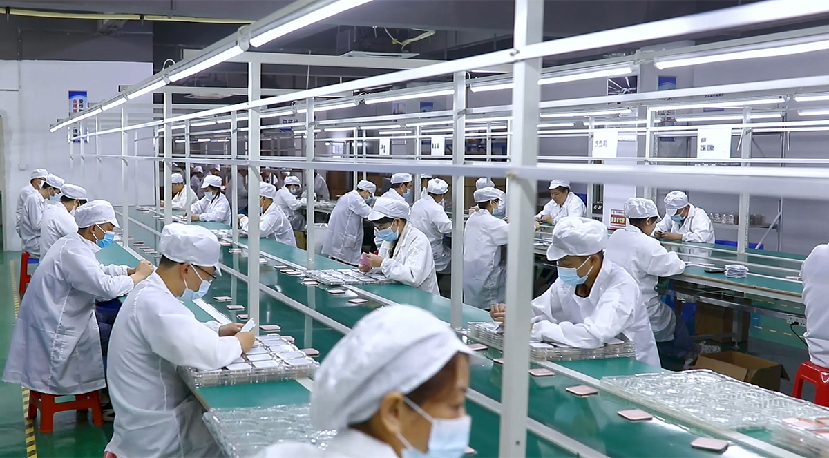
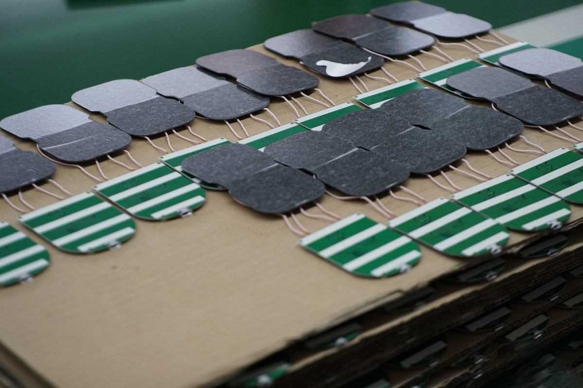
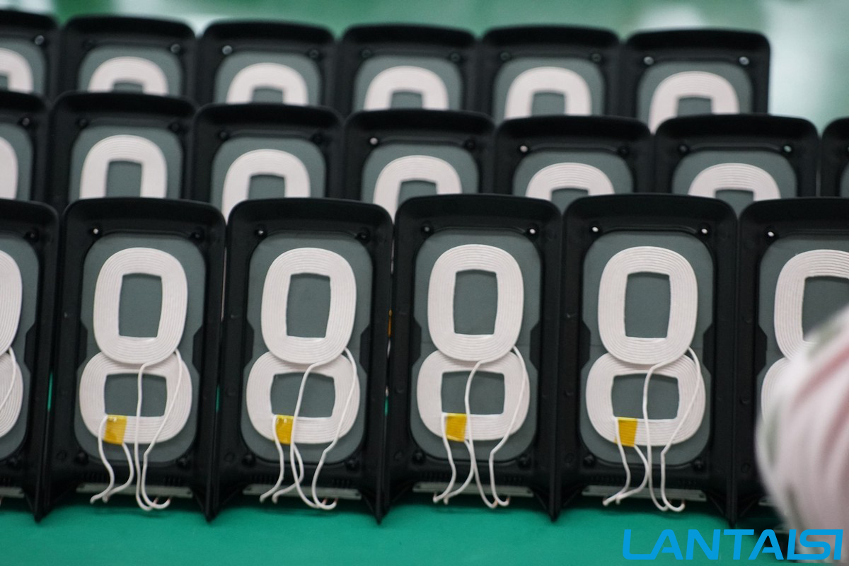
Step 6 : The qualified PCBA board will be sent to the next process-welding the transmitter coil.
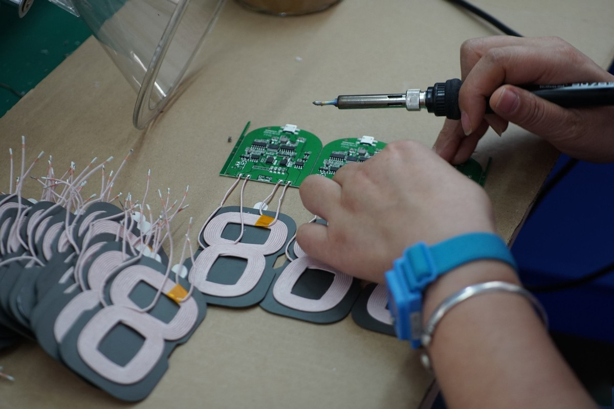
Step 7 : Welding the transmitter coil requires manual operation. It can be seen from the picture that the technician has a blue wristband on his left hand. There is a wire on this wristband that is grounded to prevent human body static electricity from penetrating the high-precision chip.
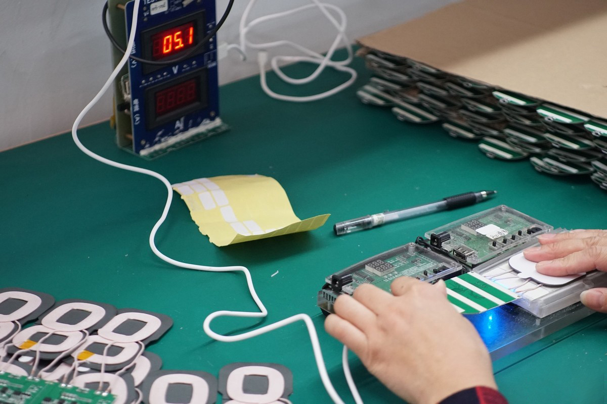
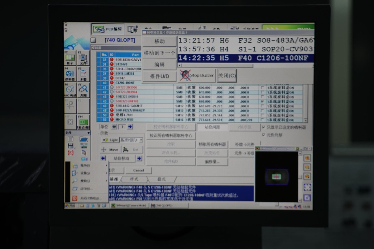
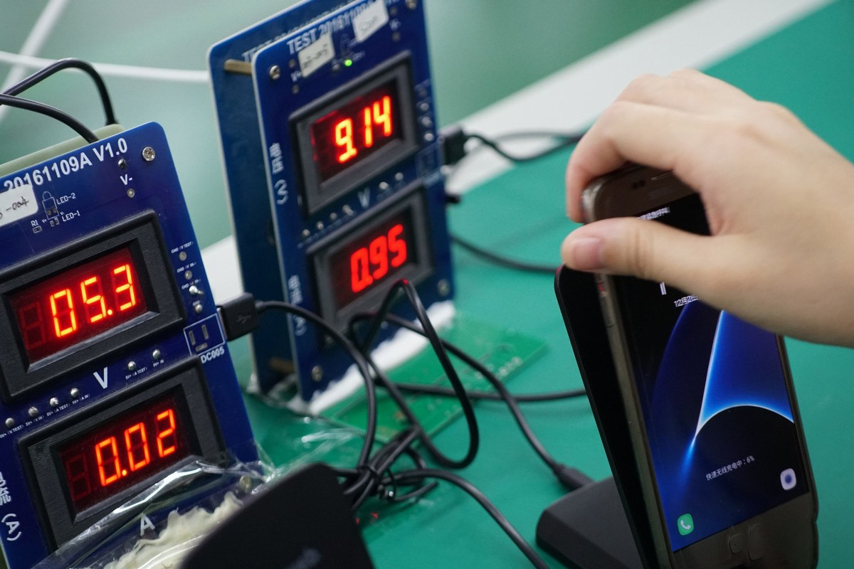
Step 8 : Next, check whether the transmitter coil board can work normally. Here, the working conditions of different input voltages will be tested.
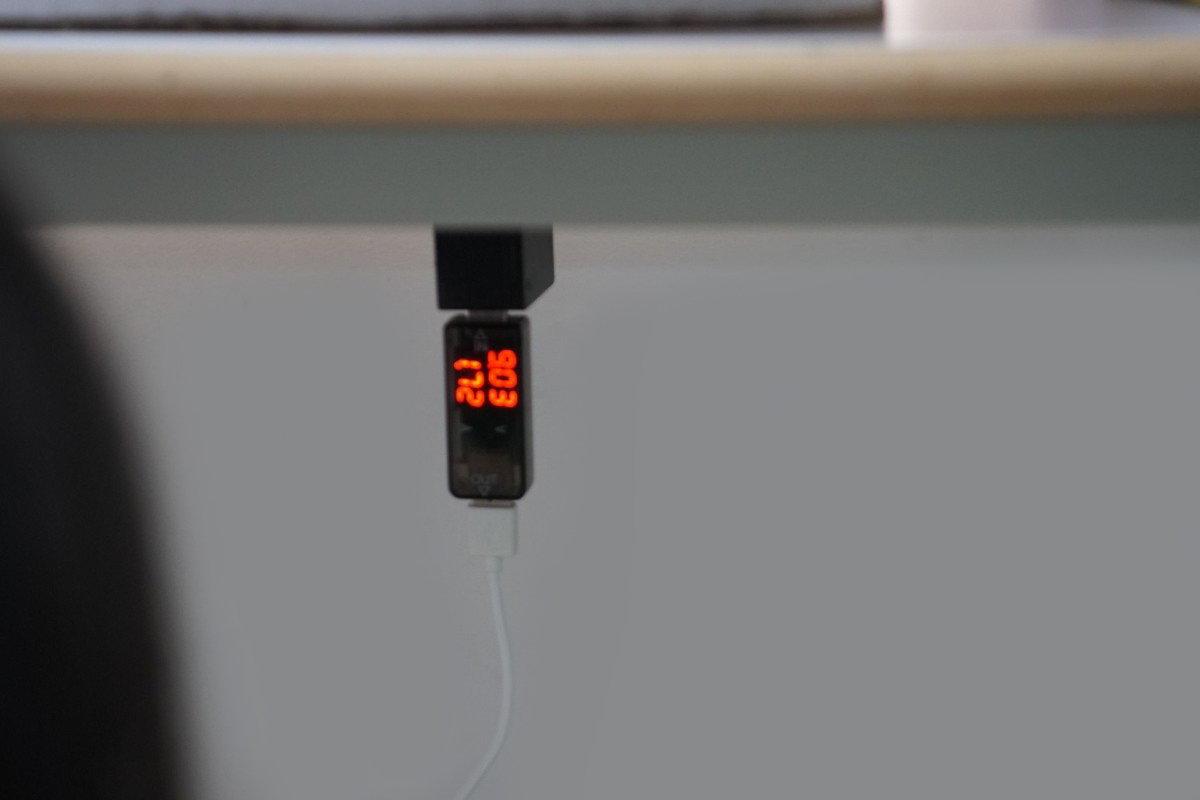
(The picture above shows the voltage and current when the wireless charger is fast charging, 9V/1.7A.)
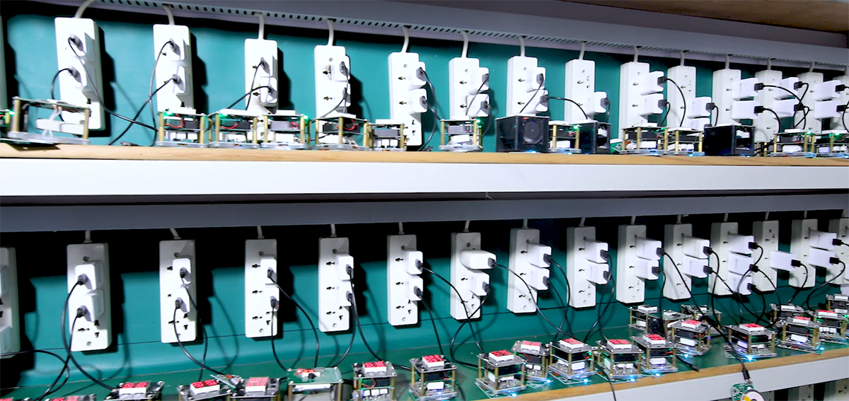
Step 9 : This process is an aging test. Each qualified wireless charger needs to be tested for power and load before leaving the factory, so that defective products can be screened out in advance during the test process; those that pass the aging test will enter the assembly process, and the defective ones will be Extract it to troubleshoot the problem. According to the factory engineer, the single-coil wireless charging requires a 2-hour aging test, while the dual-coil is 4 hours.
The picture above shows the wireless charging circuit board after aging test, and each piece is neatly arranged. The ones with the electronic components face down to avoid damaging them during the bumping process.
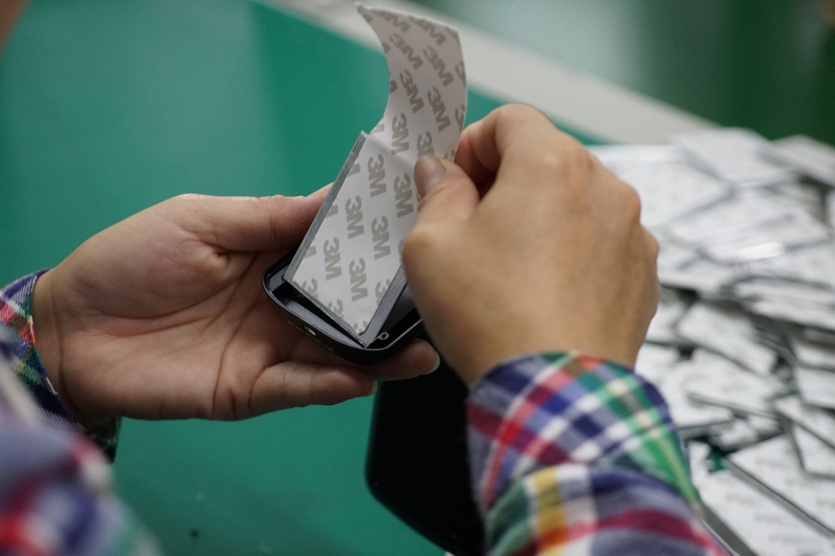
Step 10 : Fix the transmitter module on the wireless charger shell with 3M glue.
The above picture shows the semi-finished wireless charger that has been assembled and is about to wait for the next assembly link.
Step 11 : Fasten the screws.
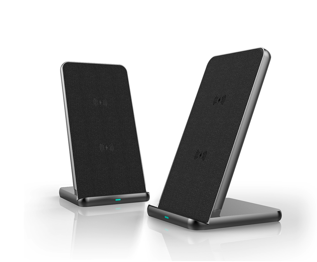
A vertical wireless charger with dual-coil fast charging is complete.
Step 12 : Finished product testing before shipment. This link is used to eliminate the compatibility of wireless charging, and to ensure that the wireless charging product that arrives in the user’s hand can have the same performance experience as the original charger.
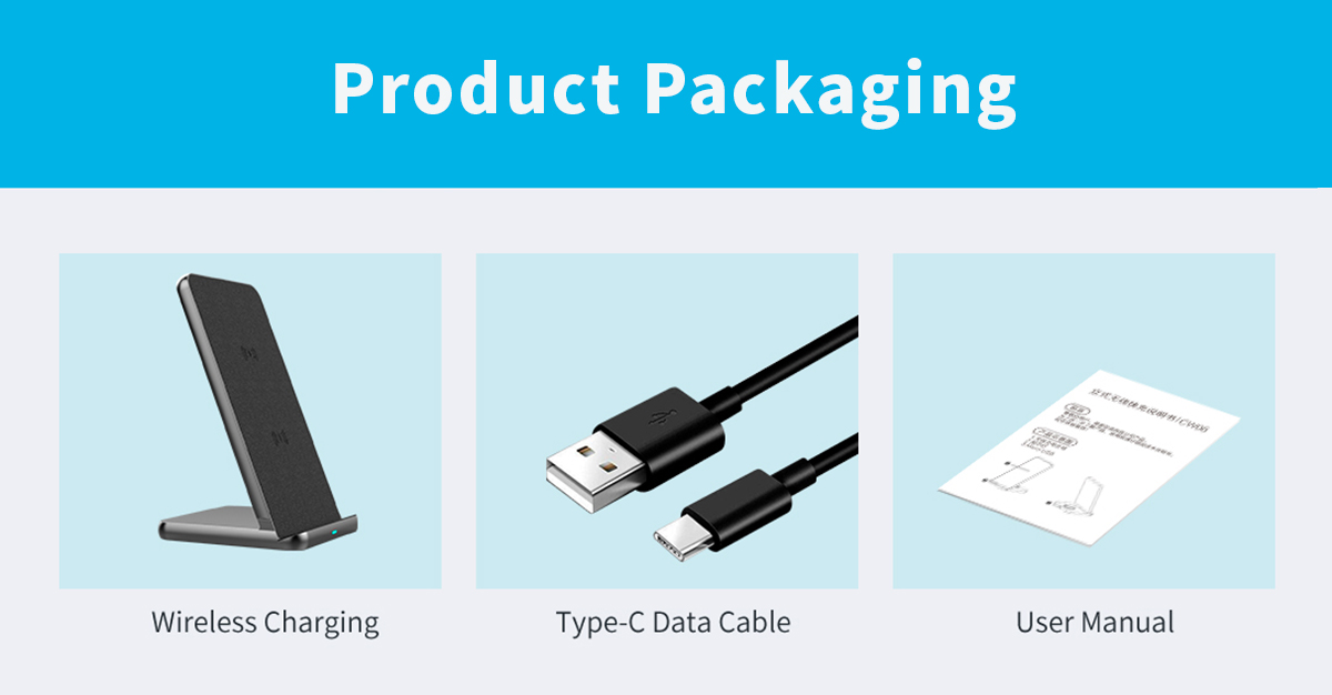
Step 13 : Put the product in a PE bag, put it in the manual, Type-C data cable, and pack it in a box, then pack it and wait for shipment.
The above is the complete production process of wireless charging. In short, it is blank board printing, SMT patch, reflow soldering, PCBA inspection, soldering coil, inspection, aging test, glue, shell assembly, finished product test, and finished product packaging.
(Of course, in order to ensure the safety and reliability of our products, we will conduct mold testing, electronic performance testing, appearance testing, etc., for wireless charging.)
After reading it, do you have a detailed understanding of the mysterious production process of wireless charging? For more details, please contact Lantaisi, we will be at your service within 24 hours.
Post time: Sep-25-2021